
Oxide Epiwafers & Nanoarrays
Nanovation’s oxide semiconductor technology platform spans a wide range of photonics, electronics, and nanostructured applications. Unlike conventional semiconductor platforms, oxides provide access to combinations of wide and ultra‑wide bandgaps, intrinsic material stability, and diverse crystal structures, enabling distinctive property sets, device concepts, and operating regimes that are difficult to realise using standard silicon or III‑nitride technologies.
A central feature of Nanovation’s approach is its ability to engineer oxide materials beyond standard specifications, enabled by specialised in‑house growth tools and processes, rather than reliance on commodity wafers or fixed material recipes. Through this tightly controlled epitaxial growth and structuring, the platform enables the precise tailoring of material properties to targeted applications, offering characteristics that are challenging to reproduce within mainstream manufacturing environments.
Over more than two decades, Nanovation has refined this manufacturing approach across multiple application‑driven use cases, ranging from sensing and imaging to electronic and energy‑related devices.
ZnO, NiO & Ga2O3 Epilayers (up to 3 inches in diameter)
On various substrates: 
- sapphire (c, a & m) (Data sheet)
- Si ( (100) & (111) ) (Data sheet)
- SiC (6H)
- ZnO
- GaN
- glass
- polymer
- steel
- FTO
- quartz
- paper
- etc.
Metallic Nanoparticle Arrays
- Au
- Ag
- Pt
- etc.
ZnO Nanostructure Arrays
- Multiple morphologies and configurations
- Custom geometries available


- Various forms: contact us with your specific needs (Data sheet).
Other Materials
- MgO
- p-Cu2O
- Al2O3
- ZnS
- CuO
- etc. (upon request)
Services
Nanovation supports partners across the full materials and device development chain:
- Bespoke oxide material development
- Semiconductor device prototyping and test (including laser dicing)
- Laser Lift-Off
- Epitaxial Lift-Off
- Materials characterisation:
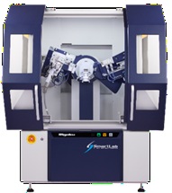
- XRD
- Hall measurements
- wafer inspection
- optical spectroscopy
- thickness measurements
Consulting
- Nanotechnology
- Compound Semiconductors
- Transparent/Flexible Electronics
- UV Sensors/Emitters
- Power Electronics
- Photovoltaics
- Oxide Materials
Get in Touch
If you have specific material requirements or would like to explore collaborations, please contact us to discuss your needs.