
Sensing Capabilities
Nanovation’s optical sensing activities are structured around four complementary development axes, all based on the same discrete (Al)Ga₂O₃ photodetector technology, and reflecting a logical progression from device‑level sensing to array‑level proof‑of‑concepts and system‑level implementation:
- Discrete solar‑blind UVC photodetectors (TRL 7–8)
- UVC imaging systems based on detector arrays (TRL 5–6)
- Discrete X‑ray and high‑energy photon detectors (TRL 3–4)
- X‑ray detection array proof‑of‑concept (TRL 2–3)
This structure reflects both the relative maturity of each activity and their position within Nanovation’s sensing roadmap.
1. Discrete Solar-Blind UVC Photodetectors (TRL 7-8)
Nanovation develops and characterises (Al)Ga₂O₃‑based solar‑blind UVC photodetectors addressing applications that require intrinsic spectral selectivity, very low dark signal, and stable electrical behaviour.
Electrical performance and reproducibility
- Dark signal: typically in the pA range under nominal operating bias, and below measurable noise levels for certain device configurations
- Spectral selectivity: intrinsic solar blindness with UVC/near‑UV rejection ratios > 10³ and UVC/visible rejection ratios > 10⁵, without the need for external optical filtering
- Reproducibility: highly consistent electrical and optical performance across full wafers and packaged batches, enabling reliable binning of devices
Temporal response and stability
- Time response: fast and reproducible rise and fall times suitable for dynamic UVC sensing
- Short‑term stability: continuous illumination tests demonstrating < 1 % variation in responsivity over several hours
- Operational repeatability: stable photoresponse under repeated illumination cycling
Taken together, these characteristics support advanced UVC sensing where background rejection and signal fidelity are critical.
→ UVC photodetector specifications (PUVC220)
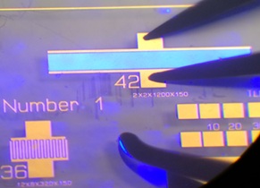
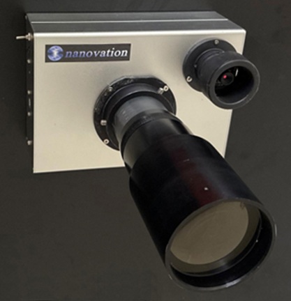
2. UVC Imaging systems Based on Detector Arrays (TRL 5-6)
Building directly on the discrete UVC photodetector technology described above, Nanovation develops UVC imaging systems based on arrays of (Al)Ga₂O₃ photodetectors.
These activities do not introduce new sensing physics; instead, they extend the same discrete detectors to array‑level and system‑level implementations.
System‑level capabilities
UVC imaging demonstrators enable:
- evaluation of uniformity and reproducibility across detector arrays
- system‑level assessment of noise, background rejection, and readout behaviour
- identification and mitigation of array‑level non‑idealities such as crosstalk
- validation of sensing concepts under application‑relevant optical conditions
These systems correspond to TRL 5–6, with remaining development risks primarily related to integration, scaling, and system engineering, rather than the underlying sensing principle.
3. Discrete X-Ray and High energy Photon Detectors (TRL 3-4)
In parallel with UVC activities, Nanovation develops (Al)Ga₂O₃‑based discrete detectors for X‑ray and high‑energy photon detection, with a particular emphasis on ultra‑low‑dose sensitivity.
Low‑dose detection capability
These detectors exhibit:
- exceptionally low dark signal and noise levels
- high sensitivity under low photon flux conditions
This performance regime approaches or exceeds the state‑of‑the‑art for solid‑state wide‑bandgap X‑ray detectors, enabling detection in scenarios where dose minimisation or photon scarcity is a critical constraint.
Envisaged application domains
Such low‑dose capability opens pathways toward:
- medical and biomedical X‑ray detection, where patient dose reduction is essential
- soft X‑ray and low‑flux scientific instrumentation
- non‑destructive evaluation of radiation‑sensitive or fragile materials
At present, these activities correspond to TRL 3–4, with device concepts and architectures validated at laboratory level.
4. X-Ray Detection Array Proof-of-Concept (TRL 2-3)
Beyond discrete detector development, Nanovation has demonstrated a monolithic multi‑pixel X‑ray detection array, implemented as a 4 × 4 (Al)Ga₂O₃ sensor architecture and experimentally evaluated at pixel level.
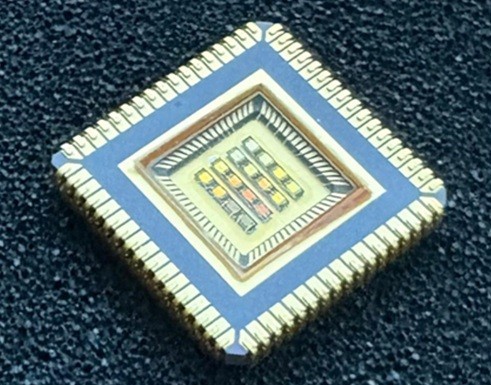
In this configuration:
- individual pixels within a monolithic array were addressed and tested
- early array‑level behaviour and operability were experimentally assessed
At this stage, the activity represents an array‑level proof‑of‑concept rather than a complete imaging system.
Key developments remaining include:
- dedicated array‑level packaging
- optical and mechanical integration
- array‑specific readout and interconnection architectures
- extended electrical and functional testing at assembly level
The current maturity therefore corresponds to TRL 2–3, bridging technology concept formulation and experimental proof‑of‑concept at the monolithic array scale.
Application Evidence
The sensing capabilities described above underpin a range of application studies documented in use‑case publications, including:
- solar‑blind UVC sensing and imaging for fire and flame detection
- UVC communication and line‑of‑sight‑independent optical signalling
- environmental and atmospheric UVC monitoring
- low‑dose and high‑energy photon detection in scientific instrumentation